Fast synthesis of PbS nanoparticles for fabrication of glucose sensor with enhanced sensitivity
Tác giả: ĐH Quốc tế Bắc Hà
Bài báo khoa học về lĩnh vực Vật lý, có sự tham gia nghiên cứu của thạc sĩ Nguyễn Xuân Quy, ĐH Quốc tế Bắc Hà
//link.springer.com/article/10.1007/s11664-016-5278-7
Cong Doanh Saia, Manh Quynh Luua, Van Vu Lea, Phuong Mai Nguyena, Nguyen Hai Phama, Viet Tuyen Nguyena,*, Xuan Quy Nguyenb,Quoc Khoa Doanc,#,Thi Ha Trand
aFaculty of Physics , Vietnam National University – University of Science, 334 Nguyen Trai, Thanh Xuan, Hanoi, Vietnam
b Bac Ha International University, Lim town, Tien Du district, Bac Ninh province.
cDuy Tan University, 182 Nguyen Van Linh, Danang, Vietnam.
dFaculty of General Sciences, Hanoi University of Mining and Geology, Tu Liem, Hanoi, Vietnam
Corresponding author:
Email: *[email protected]; #[email protected]
Tel: +84 4 35583980; Fax: +84 4 3858 4069
Abstract:
PbS nanoparticles of 12 nm in average size were synthesized by a novel time-saving method, which is the combination of the sonochemical method and laser post-annealing process. Laser annealing proved an important step in improving crystal quality of the nanoproduct. The PbS nanoparticle’s crystalline quality and morphology were characterized with several techniques such as Raman spectroscopy, X-ray diffraction, transmission electron microscopy, diffuse reflectance spectroscopy and energy dispersive X-ray analysis. The as-produced PbS nanoproduct was then used to make a glucose sensor. Electrochemical measurements showed that the sensitivity of the glucose sensor based on PbS nanoparticles was 546.2 μAcm-2mM-1, which is much higher than the glucose sensors based on other semiconductor materials reported in literature.
Keywords: Lead sulfide; Nanoparticles; Laser annealing; Sonochemical; Glucose sensor.
- Introduction.
As an important semiconductor of the IV-VI group, lead sulfide (PbS) has attracted considerable attention due to its unique properties such as a small direct band-gap (0.41 eV at 300 K) and large Bohr exciton radius of 20 nm [1, 2]. PbS has been widely used for a long time in many electronic applications such as sensors, phototransitors, and solar absorbers, etc [3, 4, 5]. During the past several decades, the interest of PbS to material scientists and engineers has shifted to the fabrication of nanostructures thanks to their enhanced surface and quantum properties, which cannot be attained by its bulk counterpart. Different methods were utilized to fabricate PbS nanostructures, for example: chemical deposition, electro-deposition, photochemical method and vacuum deposition, etc... [6-13]. Among these methods, solution growth techniques by the general or sonochemical method in particular showed some advantages, which included low cost, high efficiency, and ease of scaling production. However, such methods did not always offer high quality products. In this paper, we present a fast and convenient process combining sonochemical synthesis and laser treatment in order to produce high quality PbS nanoparticles efficiently. The average size of the as-prepared PbS was approximately 12 nm. The products were characterized by X-ray powder diffraction (XRD), Raman spectroscopy, transmission electron microscopy (TEM), high resolution transmission electron microscopy (HRTEM), selected area electron diffraction (SAED) and diffuse reflectance spectroscopy. A glucose sensor was then fabricated based on the obtained PbS nanoparticles. The sensor was characterized by electrochemical measurements, which showed high sensitivity. These results suggested that PbS nanoparticles would be very promising for fabrication of low cost, high sensitivity glucose sensors. - Experiment
Lead sulfide nanoparticles were synthesized by sono-chemical method followed by post annealing using laser. The starting chemical regents were Pb(CH3COO)2 99%, thioacetic acid (TAA) 99% andcetyltrimethylammonium bromide (CTAB) 99,8%. The chemical regents were from Merck (Germany) and used without any further purification. In a typical process, 20 ml Pb(CH3COO)2 0.25 M, 20 ml TAA 0.6 M and 10 ml CTAB 0.06 M were mixed together. The solution was ultra-sonicated by using a titanium horn(A VCX 750 ultrasonic generator, 20 kHz). The reaction took place in a nitrogen ambient atmosphere to minimize any oxidation that could affect the product. After 10 min, a black precipitate formed and was collected by a centrifugation process. After being washed and dried, the product was post-annealed using a 632.8 nm laser beam in vacuum to prevent the product from being oxidized. The annealing process was performed in several cycles, each of which lasted for 30s.
The evolution of crystal structure of the PbS nanoproduct during annealing was observed by Raman spectroscopy (Horiba Labram HR800) with an excitation wavelength of 632.8 nm. The crystal structure of the PbS nanoproduct was analyzed by using an X-ray diffractometer (Siemens D5005, Bruker, Germany) with Cu-Kα1 (λ= 0.154056 nm) irradiation. The morphology of the nanoparticles was characterized by using a high resolution transmission electron microscope (FEI Tecnai TF20 FEG). The composition of the sample was determined by energy dispersive X-ray (EDX) spectrometry (Oxford Isis 300) integrated in a JEOL-JSM 5410 scanning electron microscope. Diffuse reflectance spectra of the PbS powder were collected by using an UV-Vis-NIR Cary 5000 spectrophotometer.
Electrochemical measurement setup for glucose sensor.
The working electrode (WE) for the electrochemical glucose sensing measurements was a 3 mm diameter gold circular plate (Fig. 1). The electrode was cleaned with HCl 0.1M and NaOH 0.1M solutions in sequence. A drop of polystyrene (PS) in dichloromethane (CH2Cl2) containing 400 units glucose oxidase (GOx) and 1mg PbS was then dropped onto the electrode. After the CH2Cl2 had completely evaporated, a PbS/GOx/PS thin film was formed, and severed as an electron receptor.
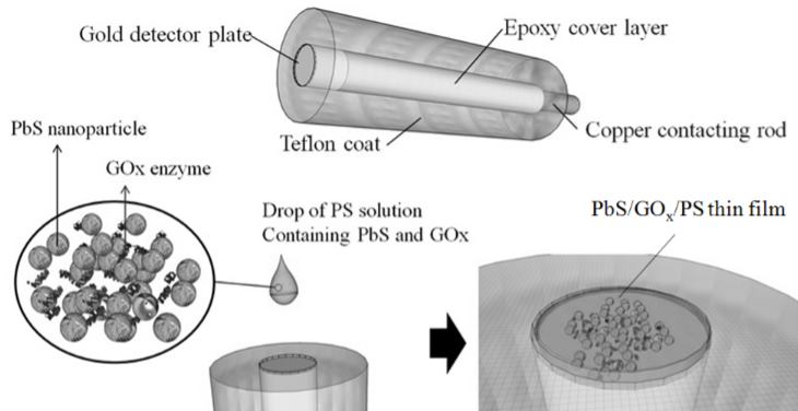 Fig. 1. Schematic diagram of PbS/GOx/PS working electrode.
- Results and discussion
PbS is sensitive to photodecomposition, meaning that PbS nanoparticles could be turned into other substances related to oxygen such as PbO or lead sulfate, according to Yousefi et al. [15] and Blackburn et al. [16]. To eliminate the possibility of photodegradation due to laser annealing, the laser treatment was performed in a vacuum chamber in several cycles, each of which lasted for 30s. After each cycle, the sample was examined by Raman spectroscopy in situ. The power density used in the Raman measurements was also kept low to avoid heating during the acquisition time. The evolution of the Raman spectra of the PbS nanoparticles during laser annealing is shown in Fig.2. Only one sharp peak at 133 cm-1 was observed, which could be assigned to either the vibration mode of PbO [17] or a combination of the transverse acoustic (TA) and transverse optical (TO) phonon modes of PbS [18]. As the annealing process and Raman measurements were performed in vacuum, the first explanation is not likely suitable. The missing Raman characteristic peak around 960 cm-1 of lead sulfate, which usually accompanies lead oxide [16], supports the assignment of the observed Raman peak to the vibration of the PbS lattice. In addition, the exclusion of the formation of PbO or PbSO4 was confirmed by XRD and EDX measurement of the annealed sample. As seen from the Raman spectra in Fig. 2, the crystal quality of the sample clearly improved after the first cycle and continued to grow after several following cycles. Raman intensity almost reached saturation after 6 cycles, suggesting that treatment could be finished after 3 min.
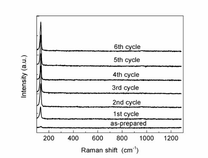 Fig. 2. Evolution of Raman spectra of PbS nanoparticles during laser annealing process.
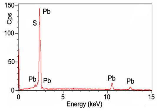 Fig. 3. XRD patterns of PbS nanoparticles before and after laser treatment.
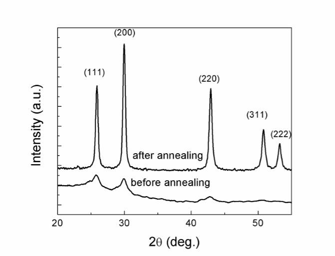 Fig. 4. EDX spectrum of PbS nanoparticles after laser annealing.
Also important to note is that no peaks related to PbO or PbSO4 was observed for the annealed sample, so the formation of unwanted phases such as PbO and PbSO4 was excluded. The lattice constant of the final product, determined from the XRD pattern, is a = 5.93(3) Å and is in good agreement with the value of 5.936 Å as reported in JCPDS-ICDD1993, No.5-592. A crystal size of about 11 nm was obtained from Debye – Scherrer relation [19]:
 L = 0.9 λ / Bcosθ (1)
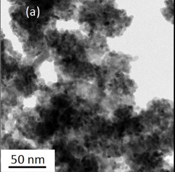
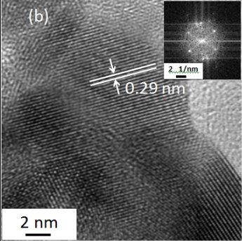
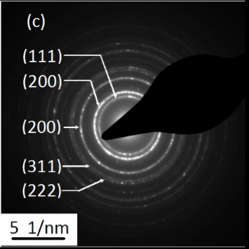 Fig. 5.(a) TEM and (b) HRTEM images and (c) SAED image of the PbS nanocrystals. The inset in (b) is the fast Fourier transform pattern of the HRTEM image.
The absorption of the PbS samples is obtained from the diffuse reflectance values by using the Kubelka-Munk function [20]:
 F(R) = (1-R)2/ 2R = K/S (2)
 αhv= A(hv – Eg)1/2 (3)
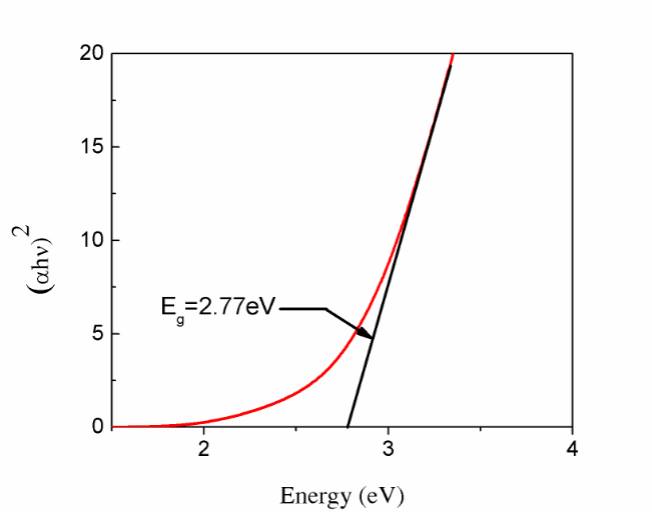 Fig. 6.The plots of (αhν)2 versus hν of the PbS nanopowders.
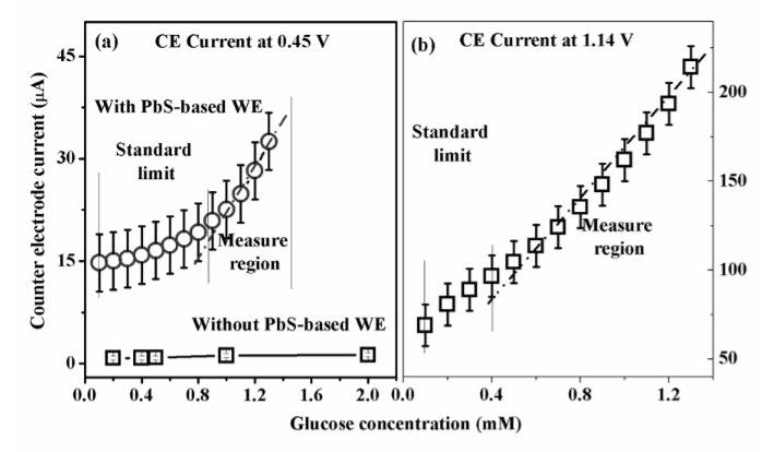
Cathodic currents at 0.45 V of the oxidation curves of different glucose concentrations with and without PbS-modified electrode are presented in Fig. 9a as a function of the glucose concentration. The dependence of the anodic current at 1.14 V from the reduction curve on the glucose concentration is shown in Fig. 9b. It should be noted that with the presence of PbS nanoparticles modified the electrode, the rise in the cathodic current at 0.45 V was much greater than when PbS was not used. Besides, the peak current at 1.14V showed higher sensitivity to glucose than the peak at 0.45 V. The sensor sensitivity, calculated from the intensity increase of 1.14V peak, was 546.2 μAcm-2mM-1. This is a high sensitivity in comparison with previous reported data [24-30].
The GOx molecules are usually found to be 580 – 585 residue long and have 3 sulfur atoms (S) containing hydrophilic cysteine at 164th, 206th and 512th positions. The 512th position is near the edge of the N-domain and close to the flavin adenine dinucleotide linking position. A possible mechanism responsible for the increase in the sensitivity of the biosensor would be a direct transfer of an electron from the mediator-materials to the molecules. Meanwhile, metal sulfide nanocrystals could easily link to the S atom of the organic molecules with a stable covalent bond [31]. The direct linkage of the material to the S atom from 512th residue could possibly induce the electron-transfer from GOx to the electrode and consequently explained the sensitivity enhancement in this report.
- Conclusion
Acknowledgement
The research was financially supported by Asia Research Center, Vietnam National University, Hanoi via Project CA.16.02A. The authors would like to thank the Faculty of Physics, Vietnam National University – University of Science for letting us use the equipment. One of the authors, Mr Sai Cong Doanh, would like to thank Project 911 of Vietnam International Education Department Fellowships for supporting his Phd tuition fee.
References
[1] O. Madelung, U. Rössler, M. Schulz, Non-Tetrahedrally Bonded Elements and Binary Compounds I, 1st edn. (Springer-Verlag, 1998), pp 874-889
[2] A. H. Khan, U. Thupakula, A. Dalui, S. Maji, A. Debangshi, S. Acharya, J. Phys. Chem. C 117, 7934 (2013)
[3] , , , , 759, 51 (2015)
[4] , , , , Sens. Actuators A 220, 213 (2014)
[5] W. Yoon, J. E. Boercker, M. P. Lumb, D. Placencia, E. E. Foos, J. G. Tischler, Sci. Rep. (2013) doi:10.1038/srep02225
[6] J. H. Warner, E. Thomsen, A. RWatt, N. R. Heckenberg, H. Rubinsztein-Dunlop, Nanotechnology 16, 175 (2005)
[7] L. Xu, W. Q. Zhang, Y. W. Ding, W. C. Yu, J. Y. Xing, F. Q. Li, Y. T. Qian, J. Cryst. Growth 273, 213 (2004)
[8] S. M. Lee, Y. W. Jun, S. N. Cho, J. W. Cheon, J. Am. Chem. Soc. 124(38), 11244 (2002)
[10] N. B. Egorov, L. P. Eremin, V. F. Usov, A. M. Larionov, High Energy Chem. 41, 251 (2007)
[11] , , , , , , 121, 19 (2014)
[12] , , , Mater. Sci. Semicond. Process. 41, 270 (2016)
[13] N.I. Fainer, M.L. Kosinova, Yu.M. Rumyantsev, E.G. Salman, F.A. Kuznetsovh, Thin Solid Films,280, 16 (1996)
[14] , , Mater. Sci. Semicond. Process. 46, 6 (2016)
[15] R. Yousefi , M. Cheraghizade, F. Jamali-Sheini, W. J. Basirun, N. M. Huang, Curr. Appl. Phys. 14, 1031 (2014)
[16] J. L. Blackburn, H. Chappell, J. M. Luther, A. J. Nozik, J. C. Johnson, J. Phys. Chem. Lett. 2, 599 (2011)
[17] R. Sherwin, R. J. H. Clark, R . Lauck, M. Cardona, Solid State Commun. 134, 565 (2005)
[18] C. Huaqiang, W. Guozhi, Z. Sichun and Z. Xinrong, Nanotechnol. 17, 3280 (2006)
[19] B. E. Warren, X-ray Diffraction, 1st edn. (Dover publications, New York, 1990), pp. 253-254
[20] N. N. Yamashita, J. Phys. Soc. Jpn. 35, 1089 (1973)
[22] R. Madhu, B. Devadas, S. M. Chen, M. Rajkumar, ACS Anal. Methods 6, 9053 (2014)
[23] , , , , ,Surf. Eng. Appl. Electrochem. 48(3), 193 (2012)
[24] , , , , , , , , Appl. Phys. Lett. (2006) doi: 10.1063/1.2356307
[25] J. Zang, C. M. Li, X. Cui, J. Wang, X. Sun, H. Dong, C. Q. Sun, Electroanalysis,19, 1008 (2007)
[26] , , Biosens. Bioelectron. 22, 2989 (2007)
[27] D.H.Yang, N. Takahara, S. W. Lee, T. Kunitake, Sens. Actuat. B-Chem. 130, 379 (2008)
[28] C. Li, Y. Liu, L. Li,Z, Du,S. Xu, M. Zhang, X. Yin, T. Wang, Talanta 77, 455 (2008)
[29] A. Umar, M. M. Rahman,Y. B. Hahn, Electrochem. Commun. 11, 1353 (2009)
[30] L. C. Jiang, W. D. Zhang, Biosens. Bioelectron. 25, 1402 (2010)
[31] N. T. Trang, L. M. Quynh, T. V. Nam, H. N. Nhat, Surf. Sci. 608, 67 (2013)
Figure captions:
Fig. 1. Schematic diagram of PbS/GOx/PS working electrode.
Fig. 2. Evolution of Raman spectra of PbS nanoparticles during laser annealing process.
Fig. 3. XRD patterns of PbS nanoparticles before and after laser treatment.
Fig. 4. EDX spectrum of PbS nanoparticles after laser annealing.
Fig. 5.(a) TEM and (b) HRTEM images and (c) SAED image of the PbS nanocrystals. The inset in (b) is the fast Fourier transform pattern of the HRTEM image.
Fig. 6.The plots of (αhν)2 versus hν of the PbS nanopowders.
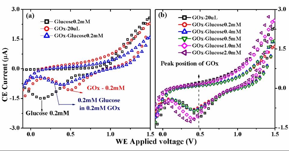
Fig. 7. Role of glucose oxidase (GOx) investigated by Cyclic Voltammetry. (a) CV diagrams of 0.2 mM Glucose, 0.2 mM GOx and 0.2 mM glucose in 0.2 mM GOx containing solution. (b) CV diagrams of different concentrations of glucose:0.2 mM, 0.4 mM, 1 mM and 2 mM in 0.2 mM GOx. All the CV measurements wereperformed with gold working electrode.
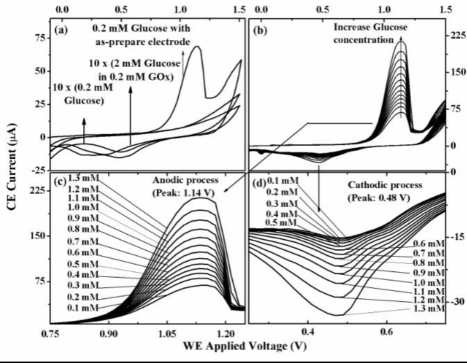
Fig. 8.CV investigation of PbS nanoparticles based WE at different glucose concentrations. (a)CV diagrams of 0.2 mM glucose, 2 mM glucose in 0.2 mM GOx with gold WE and of 0.2 mM glucose with the PbS based WE. (b) – CV diagrams of glucose solution at different concentrations – from 0.1 mM to 1.3 mM – with PbS-based WE. (c, d) – Selected regions from Anodic process and Catodic process taken from the CV diagrams in (b).
Fig. 9. Glucose concentration dependence of CE current at 0.45 V – evaluated from the CV diagrams observed with and without PbS-based electrode (a) and at 1.14 V – from the CV diagram observed with PbS-based electrode (b).

- Một số giải pháp nâng cao hiệu quả hoạt động sáng kiến, cải tiến kỹ thuật trong việc tăng cường chất lượng thực hành cho sinh viên
- 10 sự kiện Khoa học và Công nghệ nổi bật trong năm 2015
- Đề tài: Xử lý bã cafe làm phân hữu cơ vi sinh
- Máy phát điện thủy khí ACBell
- Việt Nam phát triển điện mặt trời theo hình thức nào là phù hợp
- Đề tài: Máy bơm nước bằng điện mặt trời
- Nghiên cứu lựa chọn và ứng dụng các giải pháp hợp lý áp dụng cho lưới điện phân phối việt nam đạt tiêu chuẩn lưới thông minh, mã số: kc.05.12/11-15
- Nghiên cứu khảo sát Lập bản đồ đánh giá thổ nhưỡng, khí hậu của một số vùng cây đặc sản của địa phương từ đó xây dựng quy trình chăm sóc, bảo tồn và nhân rộng Một số đặc sản
- Đề tài: Xây dựng mô hình và triển khai dự án điện mặt trời nối lưới cho các đơn vị hành chính hoặc các trường học tại các địa bàn còn gặp nhiều khó khăn
- Một số vấn đề về cơ chế tài chính với hoạt động khoa học và công nghệ ở Việt Nam
- Đầu tư trực tiếp nước ngoài ( fdi) vào Việt Nam dưới góc độ quản lý kinh tế vĩ mô
- Công trình nghiên cứu khoa học của Trường trang cá cược bóng đá trong chương trình “7 ngày công nghệ”
- Đề tài: Nghiên cứu giải pháp tổng thể trong lĩnh vực nông nghiệp sinh thái công nghệ cao phù hợp với địa hình địa lý và thổ nhưỡng của địa phương
- Đề tài: Xây dựng và triển khai dự án điện mặt trời nối lưới công suất từ 3 đến 5 KW tại trung tâm làm mô hình điểm và đánh giá kết quả. Từ đó nhân rộng trên toàn tỉnh.
- Lưới điện thông minh tại trạm biến áp hạ áp
- Ứng dụng pin mặt trời vào bơm nước và thắp sáng đèn Led cho cây trồng, vật nuôi
- Đề tài cấp Nhà nước
- Kết quả và Kết luận của khảo sát
- Đề tài nghiên cứu
- Đề tài: Mô hình tầu cao tốc có tốc độ ngang với máy bay
- Phương pháp đo nội trở để kiểm tra chất lượng ACCU - Measuring internal resistance to test battery
- Ứng dụng kỹ thuật điện tử công suất để điều khiển đóng cắt và thay đổi tham số các thiết bị bù trong lưới điện
- Sử dụng phương pháp nhúng để tăng hiệu năng của hệ vi xử lý kiến trúc OpenRISC (Using Embedding methods to increase Efficience of MicroProcessor Systems with architecture OpenRISC)
- Việt nam phát triển điện mặt trời theo hình thức nào là phù hợp
- Quy trình chế tạo IC từ phiến silicon.
- Giải pháp hữu ích: gạch định hình
- Xây dựng bài toán bù tối ưu và phương pháp thiết kế bù công suất phản kháng, nâng cao hệ số Cos
- Nghiên cứu thủ tục truy nhập đa phương tiện cho hệ thông băng thông rộng đa truy nhập theo mã và thời gian với việc sử dụng thuật toán điều khiển công suất cực tiểu và xây dựng lịch trình xử lý
Tin cùng loại

